PCB fabrication
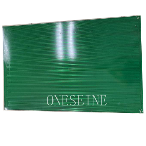
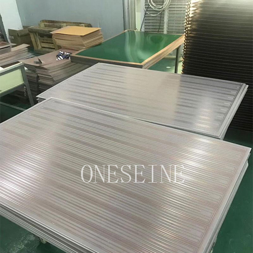
Super Long & Super Wide PCB | 800×1245mm Rogers High-Frequency Board for Transducer Applications
Super Long & Super Wide PCB | 800×1245mm Rogers High-Frequency Board for Transducer Applications
In the world of printed circuit board manufacturing, standard panel sizes typically range from 406×508mm (16×20 inches) to 508×610mm (20×24 inches). However, certain specialized applications — such as large ultrasonic transducer arrays, industrial sensor systems, and high-frequency antenna arrays — require PCBs that far exceed these conventional dimensions. A super long and super wide PCB measuring 800×1245mm represents a significant manufacturing challenge, requiring specialized equipment, precise process control, and advanced material handling capabilities.
This article explores the technical specifications, manufacturing challenges, material considerations, and application context of an extra-large Rogers PCB designed specifically for transducer applications.
1. Product Specifications Overview
This extra-large PCB is engineered for high-performance transducer systems, combining a massive board size with high-frequency Rogers substrate material. The key specifications are:
PCB Type: Super long, super wide extra-large format PCB
Board Size: 800mm × 1245mm (approximately 31.5 × 49 inches)
Base Material: Rogers high-frequency laminate
Surface Finish: Lead-free HASL (Hot Air Solder Leveling)
Copper Weight: 1 oz (approximately 35μm finished copper)
Target Application: Transducer (ultrasonic / acoustic / sensor systems)
2. Why Extra-Large Format PCBs Are Needed
Standard PCB manufacturing equipment and panel sizes are designed for typical consumer and industrial electronics. However, several application categories demand boards that exceed standard dimensions:
2.1 Transducer Arrays
Ultrasonic transducer arrays — used in medical imaging, industrial non-destructive testing (NDT), sonar systems, and acoustic levitation — often require a large, continuous substrate to accommodate hundreds or thousands of transducer elements arranged in a precise geometric pattern. A single large PCB eliminates the signal integrity and alignment issues that arise when tiling multiple smaller boards together. Each transducer element requires precise impedance control, consistent dielectric properties, and reliable interconnection — all of which are best achieved on a single, uninterrupted substrate.
2.2 Large Antenna Arrays
Phased array antennas, radar systems, and satellite communication ground stations require large aperture areas with precisely positioned antenna elements. A single large PCB ensures consistent electrical performance across the entire array, avoiding the discontinuities and connector losses associated with multi-board assemblies.
2.3 Industrial Sensor and Measurement Systems
Large-format industrial sensors — such as flat-panel inspection systems, large-area pressure sensors, and coordinate measurement systems — benefit from a single large PCB that covers the entire sensing area, reducing wiring complexity and improving measurement accuracy.
2.4 LED Lighting and Display Backplanes
Extra-large PCBs are also used in large-format LED lighting panels, stage lighting, and display backplanes, where a single board provides uniform thermal performance and simplifies assembly.
3. Rogers High-Frequency Material: Why It Matters for Transducers
The choice of Rogers high-frequency laminate is critical for transducer applications, where signal integrity at high frequencies directly impacts system performance.
3.1 Key Properties of Rogers Laminates
Rogers Corporation produces a family of high-frequency ceramic-filled PTFE (polytetrafluoroethylene) and hydrocarbon ceramic laminates, each engineered for specific frequency and performance requirements. Common Rogers materials include:
RO4000® Series (RO4003C, RO4350B, RO4360, RO4533, RO4535): Hydrocarbon ceramic laminates with low dielectric loss, designed for high-volume commercial applications. RO4350B (Dk 3.48, Df 0.0037 at 10GHz) is one of the most widely used Rogers materials for RF and microwave designs.
RO3000® Series (RO3003, RO3006, RO3010, RO3203, RO3206, RO3210): PTFE-based laminates with tightly controlled dielectric constants ranging from 3.0 to 10.2, used for high-performance RF, microwave, and millimeter-wave applications.
RO5880™: A pure PTFE-glass laminate with Dk 2.2 and extremely low loss (Df 0.0009 at 10GHz), ideal for ultra-high-frequency and millimeter-wave designs.
3.2 Why Rogers for Transducer PCBs?
Transducer systems — particularly ultrasonic and acoustic transducers — operate at frequencies ranging from hundreds of kHz to several GHz (for microwave acoustic devices). At these frequencies, the dielectric loss and signal attenuation of standard FR-4 material become unacceptable. Rogers laminates offer:
Low dielectric loss (Df): Minimizes signal attenuation and heat generation, critical for high-power transducer drive circuits
Tightly controlled dielectric constant (Dk): Ensures consistent impedance matching across the entire large-format board, which is essential for uniform transducer element performance
Low moisture absorption: Maintains stable electrical properties in humid environments
Excellent thermal stability: Dk remains stable over a wide temperature range, ensuring consistent transducer performance
Good dimensional stability: Critical for large-format boards where even small material expansion or contraction can misalign transducer elements
3.3 Rogers Manufacturing Considerations
Rogers materials differ significantly from FR-4 in processing, requiring specialized manufacturing knowledge:
Drilling: PTFE-based Rogers materials can smear and require specialized drill parameters (slower feed rates, specialized drill bit geometry) to achieve clean hole walls
Etching: Rogers copper foil may have different surface treatment, requiring adjusted etching parameters
Lamination: Multi-layer Rogers boards require controlled lamination temperature, pressure, and ramp rates to avoid delamination and resin flow issues
Solder mask: Specialized solder mask materials and application methods may be required for proper adhesion to Rogers substrates
Surface finish: Rogers materials are compatible with most standard surface finishes, including HASL, ENIG, immersion silver, and OSP
4. Manufacturing Challenges of Extra-Large PCBs
Producing an 800×1245mm PCB presents unique manufacturing challenges that go beyond standard PCB production:
4.1 Equipment Size Limitations
Most standard PCB manufacturing equipment — including exposure machines, etching lines, plating tanks, AOI (Automated Optical Inspection) systems, and electrical test fixtures — is designed for standard panel sizes. Extra-large boards require:
Large-format exposure machines with uniform light intensity across the entire 800×1245mm area to ensure consistent line width and registration
Extended etching and plating lines with uniform chemical flow and temperature across the full board width, preventing edge-to-center variation in copper thickness and etch rate
Large-format lamination presses with uniform pressure and temperature distribution to avoid delamination, resin starvation, or thickness variation
Custom electrical test fixtures or flying probe test systems capable of handling the oversized format
Specialized handling equipment to transport large, thin, or heavy boards through the production line without bending or scratching
4.2 Dimensional Accuracy and Registration
On a large-format board, even small registration errors or material dimensional changes are magnified across the 1245mm length. Key challenges include:
Layer-to-layer registration: Multi-layer extra-large boards require extremely precise alignment between layers, as any misalignment is amplified across the large format
Material dimensional change (shrinkage/expansion): Rogers materials and FR-4 can expand or contract during lamination and processing; on an 800×1245mm board, a 0.1% dimensional change equals 1.245mm of displacement — enough to cause serious via misalignment
Etch uniformity: Ensuring consistent trace width from the center to the edges of a 1245mm-long board requires tightly controlled etching parameters and uniform spray pressure
Copper thickness uniformity: Electroplating uniformity across a very large surface area is challenging; edge effects can cause thicker copper at board edges
4.3 Warpage and Flatness Control
Large-format PCBs are inherently more prone to warpage (bow and twist) due to:
Copper distribution imbalance: Uneven copper coverage across the large board causes differential shrinkage during lamination and cooling
Material CTE mismatch: Differences in coefficient of thermal expansion between copper, dielectric, and (in mixed constructions) FR-4 and Rogers materials
Gravity effects: Large, thin boards can sag under their own weight during high-temperature processing
Manufacturers control warpage through balanced copper distribution, symmetric layer stackups, controlled cooling rates, and post-lamination flattening processes. For transducer applications, board flatness is especially critical — a warped board can misalign transducer elements and degrade acoustic coupling.
4.4 Lead-Free HASL on Large Boards
The lead-free HASL (Hot Air Solder Leveling) surface finish provides excellent solderability and low cost, but applying it uniformly across an 800×1245mm board presents challenges:
The entire board must be evenly coated with molten solder (typically SnCu or SAC alloy) and then leveled with hot air knives
Large boards require longer immersion time, increasing thermal exposure — Rogers materials have specific maximum temperature limits that must be respected
Solder thickness uniformity across the large surface area must be controlled to avoid excessive solder buildup (which can affect component placement) or thin spots (which can compromise solderability)
Lead-free HASL operates at approximately 260–270°C, requiring careful thermal management to avoid board warpage or material degradation
4.5 Packaging, Shipping, and Handling
Extra-large PCBs require specialized packaging to prevent damage during transit:
Rigid packaging (wooden crates or reinforced cardboard) to prevent bending
Interleaving with protective film or foam to prevent scratching
Vertical or horizontal storage orientation depending on board thickness and rigidity
Moisture barrier packaging with desiccant for Rogers materials, which can absorb moisture over time
5. 1 oz Copper Weight: Balancing Current and Signal Integrity
The 1 oz (35μm) finished copper weight is a standard choice for this transducer PCB, offering a balance between:
Current-carrying capacity: 1 oz copper is sufficient for most transducer drive and signal circuits; for higher-power transducer elements, thicker copper (2oz or more) may be specified
Signal integrity: Standard 1 oz copper is well-characterized for impedance calculations and is compatible with fine-line geometries (typically down to 4–6mil trace/space) needed for high-density transducer element routing
Cost: 1 oz copper is the most cost-effective standard weight, helping to manage the already elevated cost of an extra-large Rogers PCB
Manufacturability: 1 oz copper is the most widely supported weight across all PCB processes, including etching, plating, and solder mask application
6. Transducer Application Considerations
For transducer applications, the PCB serves not merely as an interconnect substrate but as an integral part of the transducer system's electrical and mechanical performance:
6.1 Impedance Control
Each transducer element and its associated drive/sense trace must have a precisely controlled characteristic impedance (typically 50Ω for RF transducers, or custom values for piezoelectric ultrasonic transducers). On an 800×1245mm Rogers board, impedance consistency across all elements is critical — any variation in trace width, dielectric thickness, or Dk will cause element-to-element performance variation.
6.2 Signal Routing Density
A large transducer array may contain hundreds or thousands of individual elements, each requiring a separate signal trace. The 800×1245mm format provides the necessary area, but routing all traces to the connector(s) without crosstalk or impedance disruption requires careful layer stackup design, ground plane integrity, and trace spacing (typically following the 3W rule for high-speed signals).
6.3 Thermal Management
Transducer systems — especially high-power ultrasonic or acoustic transducers — generate significant heat. The Rogers substrate, while electrically superior, has a lower thermal conductivity than some metal-core or ceramic substrates. Thermal management may require thermal vias, copper pours, and external heat sinking to maintain operating temperatures within the transducer's and the PCB material's limits.
6.4 Mechanical Stability and Acoustic Coupling
In ultrasonic transducer applications, the PCB may be directly bonded to the piezoelectric material or acoustic matching layers. Board flatness, surface smoothness, and dimensional stability are critical for achieving uniform acoustic coupling across the entire array. Any warpage or surface irregularity can create air gaps that severely degrade acoustic transmission.
7. Conclusion
An 800×1245mm super long and super wide PCB built on Rogers high-frequency material with lead-free HASL finish and 1 oz copper represents the intersection of large-format manufacturing expertise and high-frequency material technology. Designed for transducer applications — where large aperture, precise impedance control, low dielectric loss, and dimensional stability are paramount — this type of board demands specialized production capabilities that only a select number of Chinese PCB manufacturers possess.
The key challenges — equipment size limitations, dimensional accuracy and registration across the oversized format, warpage control, uniform lead-free HASL application, and specialized packaging — all require rigorous process control and engineering expertise. When manufactured correctly, an extra-large Rogers transducer PCB delivers superior electrical performance, uniform element response, and long-term reliability that cannot be achieved by tiling multiple smaller boards.
For engineers and procurement teams evaluating extra-large high-frequency PCBs, the critical success factors are: selecting a manufacturer with proven large-format Rogers experience, defining a realistic layer stackup and impedance requirements, specifying adequate flatness and dimensional tolerances, and planning for the specialized handling and packaging that oversized boards require.
SEO Keywords
super long PCB, extra large PCB board, 800x1245mm PCB, Rogers high frequency PCB, transducer PCB, large format PCB manufacturer, oversized PCB China, lead free HASL PCB, 1oz copper PCB, ultrasonic transducer PCB, high frequency transducer board, large antenna array PCB, Rogers RO4350B PCB, extra wide PCB, big size PCB manufacturing
Categories
News
Contact Us
Contact: Flexible PCB
Phone: 0086 18682010757
E-mail: kico@oneseine.com
Add: BldB,Fushan Industrial Park,Qianwu Town,Doumen,Zhuhai,China